


In the fast-paced world of electronics manufacturing, Printed Circuit Boards (PCBs) serve as the backbone of nearly every electronic device. With increasing complexity and demand for performance, product reliability has become a non-negotiable benchmark. Leading PCB factories are meeting this challenge head-on through comprehensive in-house testing procedures designed to detect defects, ensure performance, and meet global quality standards.
Why In-House Testing Matters in PCB Manufacturing
In-house testing is crucial because even the smallest defect in a PCB can lead to failure in the final electronic product. Whether it’s a short circuit, misalignment, or signal interference, undetected flaws can compromise both functionality and safety. To mitigate these risks, top-tier PCB manufacturers invest in robust testing protocols at every stage of production.
Types of In-House PCB Testing Methods
1. Automated Optical Inspection (AOI)
AOI machines use high-resolution cameras to inspect PCBs for visual defects like soldering issues, missing components, or misalignments. It’s fast, accurate, and essential for Surface Mount Technology (SMT) lines.
2. In-Circuit Testing (ICT)
This method verifies the electrical performance of each component on the PCB. By probing individual nodes, ICT checks for shorts, opens, resistance, capacitance, and more—ensuring the board functions as designed.
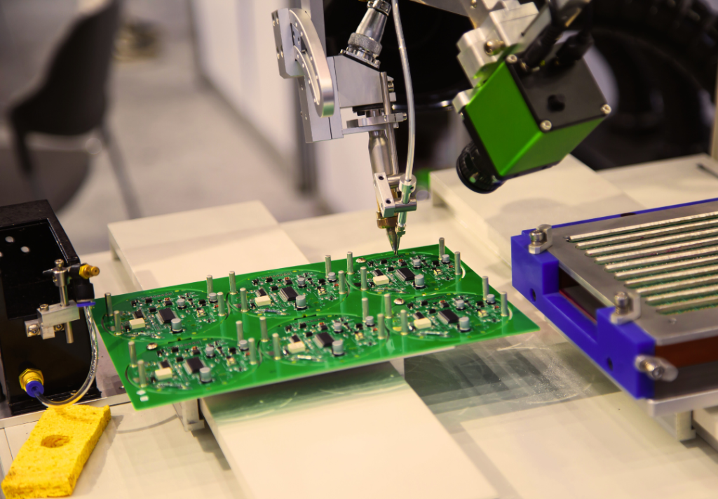
3. Flying Probe Testing
Ideal for low-to-medium volume runs, flying probe testers use robotic arms to test boards without the need for custom fixtures. It’s a flexible, cost-effective solution for prototype testing and quick-turn PCBs.
4. X-Ray Inspection
Especially important for multilayer and high-density PCBs, X-ray testing allows manufacturers to inspect hidden solder joints, such as those beneath Ball Grid Array (BGA) packages.
5. Functional Testing
In this final step, the PCB is tested under actual working conditions. This test simulates the end-use environment, verifying the board’s behavior under real-world voltage, current, and signal parameters.
Benefits of In-House PCB Testing
- Early Defect Detection: Identifies issues before boards are shipped or integrated into larger assemblies.
- Cost Efficiency: Reduces rework and warranty claims by catching problems early.
- Faster Turnaround: On-site testing streamlines production timelines and improves delivery reliability.
- Compliance Assurance: Ensures the product meets international quality standards such as IPC, ISO, and RoHS.
How Leading PCB Factories Maintain Testing Standards
Top PCB factories follow a Quality Management System (QMS) that integrates testing at multiple checkpoints throughout the production process. From incoming raw material inspection to final functional testing, every step is documented and traceable. Additionally, many facilities are ISO 9001 and IATF 16949 certified, underscoring their commitment to quality assurance.
Some factories also implement Statistical Process Control (SPC) to monitor production trends in real time and prevent defects before they happen.
Conclusion: Reliability Starts at the Factory Floor
In an industry where even a microscopic defect can lead to significant consequences, in-house PCB testing is the cornerstone of product reliability. By integrating advanced inspection technologies and stringent testing protocols, PCB manufacturers can confidently deliver high-performance boards that meet the demands of modern electronics.
If you’re sourcing PCBs, partner with a PCBA Factory that prioritizes in-house testing. It’s not just about meeting specs—it’s about delivering quality you can trust.